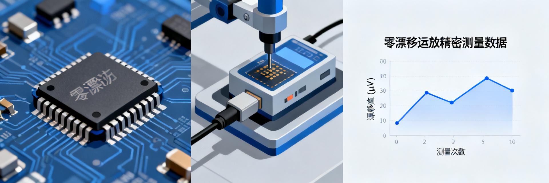
NL2333ANAE2S-ES Datasheet In-Depth Interpretation: How 5 Key Performance Parameters Enhance Precision Measurement
When precision measurement applications demand rigorous stability from the signal chain, zero-drift operational amplifiers become the core choice. The NL2333ANAE2S-ES datasheet shows a typical offset voltage of only 5µV and temperature drift as low as 0.01µV/°C. Behind this datasheet, which 5 key parameters truly determine the upper limit of precision measurement? This article will provide an in-depth breakdown based on official specifications to offer actionable selection references for R&D engineers.
In modern electronic design, signal chain accuracy directly determines the final product's performance. As the core node of the analog signal link, the choice of operational amplifier is particularly critical. A detailed datasheet is like the "DNA map" of a chip, hiding key clues that determine the success or failure of a system. Starting from the official documentation of the NL2333ANAE2S-ES, we strip away the surface and hit the core.
| Core Performance Metrics |
Typical Value (Typ) |
Significance for Precision Measurement |
| Offset Voltage (Vos) |
5µV |
Defines the system's "zero" offset, determining the absolute accuracy benchmark. |
| Temp Drift (TCVos) |
0.01µV/°C |
Extremely low thermal sensitivity, eliminating errors caused by environmental temperature fluctuations. |
| Quiescent Current (Iq) |
10µA/Ch |
Significantly enhances battery life, suitable for portable monitoring instruments. |
| Gain Bandwidth Product (GBP) |
350kHz |
Balances power consumption and speed, determining ADC front-end signal settling time. |
| Noise Handling |
Chopper-Stabilized |
Effectively eliminates 1/f noise, ensuring SNR for low-frequency signal sampling. |
Core Parameter Analysis: Why Offset Voltage and Temp Drift are the Bedrocks of Accuracy?
When it comes to precision measurement, Offset Voltage (Vos) and its Temperature Drift (TCVos) are the first hurdles that cannot be bypassed. They directly define the system's "zero" offset when there is no input signal, as well as sensitivity to temperature changes. This is not just theoretical; it is the fundamental factor determining the absolute accuracy of the measurement.
Typical vs. Maximum: Understanding the 10µV Offset Voltage Guarantee of the NL2333
In the parameter table of a datasheet, you will often see "Typical" (Typ.) and "Maximum" (Max.) columns. For example, the typical offset voltage of the NL2333ANAE2S-ES is 5µV, while the maximum is guaranteed at 10µV. This means that for every circuit you design, its initial offset voltage will not exceed 10µV. This low offset is due to its internal chopper-stabilized or auto-zero architecture. This architecture effectively eliminates the circuit's 1/f noise and thermal drift through continuous sampling and correction, ensuring that measurement results remain stable and reliable even after long hours of operation.
The Real Impact of 20nV/°C Temp Drift on High-Precision ADC Sampling
Temp drift parameters often demonstrate a device's "true capability" better than absolute offset voltage. Imagine a high-precision temperature sensor signal conditioning scenario: the ambient temperature rises from 25°C to 85°C, a difference of 60°C. Using the NL2333ANAE2S-ES typical temp drift of 0.01µV/°C, the additional offset voltage increment generated at this temperature difference is only 0.6µV. For a 16-bit ADC (reference voltage 2.5V, LSB approximately 38µV), this impact is negligible, often requiring no complex software calibration. In contrast, using a general-purpose op-amp (temp drift 5µV/°C), a 60°C difference would introduce 300µV of error, close to 8 LSBs, forcing engineers to add expensive temperature compensation circuits, which undoubtedly hinders design efficiency.
The Art of Balancing Power and Bandwidth: Performance Verification in Low-Power Scenarios
In battery-powered or portable instruments, power consumption is the primary constraint, but it must not come at the expense of signal processing capability. Balancing extremely low quiescent current with sufficient Gain Bandwidth Product (GBP) is a key measure of an excellent op-amp. The NL2333ANAE2S-ES provides an outstanding answer to this challenge.
10µA/Ch Quiescent Current: A New Benchmark for Portable Precision Measurement
The supply current vs. supply voltage curve in the datasheet shows that the typical quiescent current per channel for the NL2333ANAE2S-ES is only 10µA. This means that at a 3.3V supply, the total power consumption of the op-amp is only 33µW. Among similar precision zero-drift op-amps, this is undoubtedly a highly competitive figure. It does not achieve low power by sacrificing bandwidth. Even at such low current, it maintains excellent noise and offset performance, perfectly fitting application scenarios with extremely high battery life requirements, such as gas sensors, portable pH meters, and remote monitoring equipment.
How 350kHz Gain Bandwidth Product (GBP) Affects Signal Settling Time
Gain Bandwidth Product (GBP) determines the frequency response of the op-amp. The GBP of the NL2333ANAE2S-ES is 350kHz. In data acquisition systems, this parameter directly determines signal settling time. For example, when configured for unity gain (G=1), its -3dB bandwidth is 350kHz, and the time required for the signal to settle to 0.1% accuracy is approximately 2.2 / (2π * 350kHz) ≈ 1µs. At a gain of 10 (G=10), the closed-loop bandwidth drops to 35kHz, and the settling time extends to about 10µs. Understanding this relationship is vital for designing multiplexed sampling systems, as it helps engineers accurately estimate channel switching and stabilization times to avoid sampling errors.
Key Summary
- Core Advantage: The NL2333ANAE2S-ES datasheet reveals its core as a zero-drift op-amp, with a typical offset voltage as low as 5µV and temp drift of 0.01µV/°C, serving as the bedrock of precision measurement.
- Power Performance: The extremely low quiescent current of 10µA/Ch, combined with a 350kHz GBP, perfectly balances low power consumption with signal bandwidth needs, defining a new benchmark for portable precision measurement.
- Design Reliability: The datasheet provides detailed typical and maximum parameters, especially the 10µV maximum offset voltage guarantee, providing a solid basis for performance consistency and reliability in mass-produced products.
Frequently Asked Questions
What exactly does "Zero-Drift" mean in the NL2333ANAE2S-ES datasheet?
"Zero-drift" refers to the real-time correction of input offset voltage drift caused by temperature changes and 1/f noise through the chip's internal chopper or auto-zero circuitry. This makes the long-term and temperature stability of the NL2333ANAE2S-ES far superior to traditional op-amps, making it an ideal choice for high-precision DC or low-frequency signal measurement without the need for frequent system calibration.
How to calculate total output noise from the NL2333ANAE2S-ES datasheet?
First, find the voltage noise density curve in the manual. Next, determine your signal bandwidth. The total output noise RMS is approximately equal to the voltage noise density (nV/√Hz) multiplied by the square root of the signal bandwidth (Hz), then multiplied by the circuit's noise gain. Finally, multiply this RMS value by 6.6 to estimate the peak-to-peak (P-P) noise, which helps determine its impact on the dynamic range of the precision measurement system.
What are the precautions for using the NL2333ANAE2S-ES for precision measurement under a single-supply?
The NL2333ANAE2S-ES features Rail-to-Rail Input/Output (RRIO) characteristics, offering significant advantages under single-supply. A key precaution is to avoid the input signal getting too close to or reaching the negative supply rail (GND). Although its input stage can handle common-mode voltages including GND, linearity and offset voltage performance may degrade slightly near zero input. It is recommended to reserve a small "headroom" voltage in the circuit design, such as biasing the input signal slightly above the GND potential.
How does the GBP parameter in the NL2333ANAE2S-ES datasheet affect my ADC driver circuit design?
Gain Bandwidth Product (GBP) determines the closed-loop bandwidth of the op-amp. When driving an ADC, to ensure settling time, you need to design an RC anti-aliasing filter between the amplifier output and the ADC input. A lower GBP means a slower response speed for the op-amp, thus requiring a lower filter cutoff frequency and larger resistor/capacitor values. This perfectly matches the low-power characteristics of the NL2333ANAE2S-ES, as larger resistance values help reduce overall power consumption.