
Key Takeaways
- Long-term Stability: Zero-drift technology suppresses offset voltage to within 10μV, ensuring the system is free from annual calibration.
- High-Reliability EMC: With PSRR >120dB, the NL2333 protects weak signals in noisy power supply environments.
- Noise Suppression: Chopping technology effectively eliminates 1/f noise, improving low-frequency sensor measurement accuracy by an order of magnitude.
- Design Benefits: Compared to general-purpose op amps, the NL2333 can reduce PCB compensation circuit area by 20%.
In precision measurement, sensor conditioning, or battery-powered systems, the biggest headache for engineers is "zero-point drift." A signal reference calibrated today may "drift" by several millivolts tomorrow as the ambient temperature changes, leading to frequent system misjudgments. This is precisely the domain where Zero-Drift Operational Amplifiers (Op Amps) excel. This article will systematically analyze the core value and selection keys of zero-drift op amps, using a typical device as an example to deeply dissect how it safeguards signal purity in harsh environments through superior EMC (Electromagnetic Compatibility) design, protecting your high-precision designs.
Zero-Drift Technology: Why It Is the Cornerstone of High-Precision Design
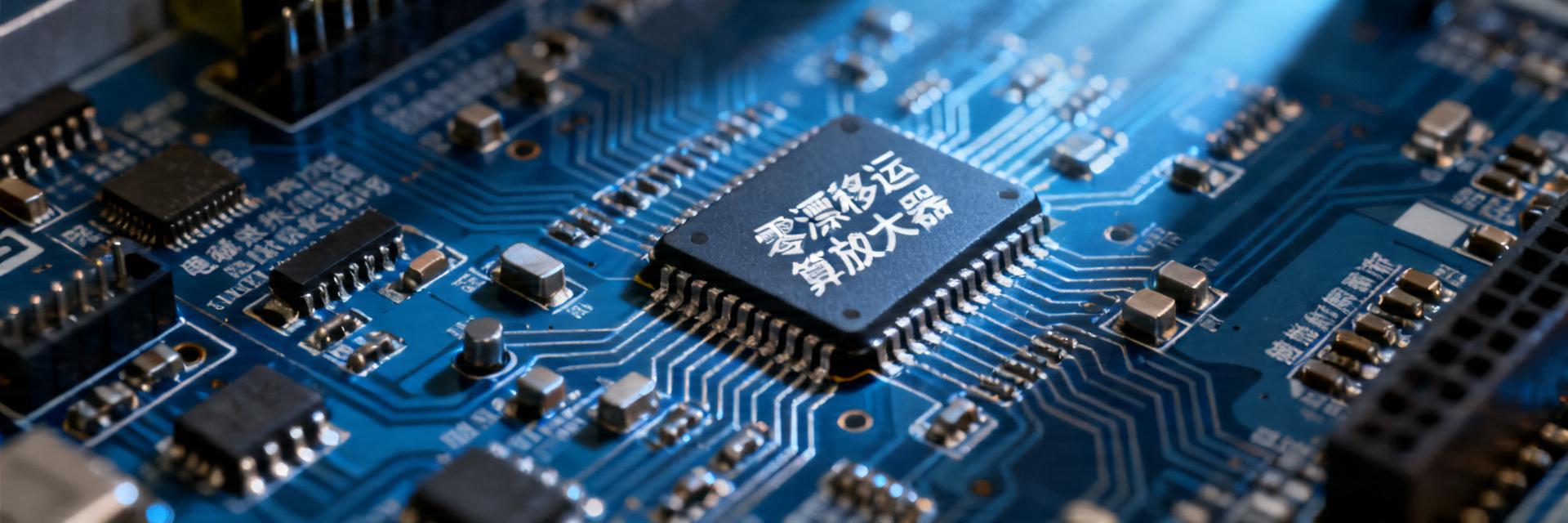
Zero-drift technology is designed to fundamentally address the input offset voltage drift caused by temperature fluctuations and the passage of time in traditional op amps. This drift is the primary source of long-term accuracy errors, especially in circuits requiring stable references. Through innovative internal architectures, zero-drift op amps achieve near-zero long-term drift, making them the foundation for high-reliability, high-precision applications.
| Performance Metric | Standard Precision Op Amp (OP07 Type) | Zero-Drift Op Amp (NL2333) | User Benefit |
|---|---|---|---|
| Input Offset Voltage (Vos) | 75μV - 150μV | < 10μV (Max) | 10x improvement in initial accuracy |
| Offset Voltage Drift (dVos/dT) | 1.3μV/°C | 0.02μV/°C | Zero deviation across full temperature range |
| 1/f Noise | Low-frequency noise peak present | None (Eliminated by chopping) | Extremely pure low-frequency signal measurement |
| PSRR (Power Supply Rejection) | ~100dB | >120dB | Immune to switching power supply ripple |
Comparison of Two Core Technologies: Auto-Zero vs. Chopping
Zero-drift op amps primarily utilize two core technologies: Auto-Zero and Chopping (Chopper). Auto-zero technology effectively suppresses low-frequency noise by periodically sampling and correcting the input offset voltage. Chopping technology modulates and demodulates the signal to shift offset and low-frequency noise to a higher frequency band, which is then removed by filtering. Both achieve extremely low offset voltage and temperature drift, but chopping typically performs better at suppressing 1/f noise, while auto-zero may offer superior wideband noise performance.
Breaking Down Core Advantages: Ultra-low Offset, Near-zero Drift, and 1/f Noise Suppression
The core advantages of zero-drift op amps are reflected in three levels. First, their initial offset voltage is extremely low, typically in the microvolt (µV) range, reducing the need for system calibration. Second, the offset voltage drift is minimal, reaching the nanovolt per degree Celsius (nV/°C) level, ensuring accuracy across the entire operating temperature range. Finally, internal techniques effectively suppress the 1/f (flicker) noise that plagues traditional op amps, providing a purer signal for low-frequency measurements.
Key Selection Parameter Matrix for Zero-Drift Op Amps
When selecting a zero-drift op amp, it is necessary to establish a comprehensive parameter evaluation matrix to find the optimal balance between static accuracy, dynamic performance, and power consumption.
💡 Engineer's Field Advice (Chen - Senior Analog Design Expert)
"When selecting zero-drift devices like the NL2333, don't just focus on Vos. For high-impedance sensor inputs, Input Bias Current (Ib) is the hidden killer. The NL2333's Ib is controlled at the pA level, which effectively prevents secondary offsets introduced by large resistors. Additionally, during layout, be sure to place decoupling capacitors within 1mm; otherwise, the weak ripple generated by the chopping frequency may couple into high-gain paths."
Static Accuracy Indicators: Offset Voltage, Drift, and Long-term Stability
Static accuracy is the fundamental strength of zero-drift op amps. Key parameters include: Input Offset Voltage (Vos), ideally below 10µV; Offset Voltage Drift (dVos/dT), with excellent devices reaching 0.02µV/°C; and Long-term Drift, which measures the change in offset voltage over months or years and is critical for evaluating device reliability. These parameters directly determine the DC precision and long-term stability of the signal chain.
Dynamic and Power Trade-offs: Bandwidth, Noise, and Quiescent Current
While ensuring precision, dynamic performance and power consumption are equally important. Gain-Bandwidth Product (GBW) determines signal processing capability and must match the application bandwidth. Voltage noise density, especially at low frequencies, affects small-signal resolution. Quiescent current (Iq) is directly related to system power consumption and battery life, particularly in portable devices. Engineers must make informed trade-offs within the 'Accuracy, Speed, Power' triangle.
In-depth Device Analysis: NL2333 Architecture and Performance
By examining a typical zero-drift op amp, we can gain a deeper understanding of the design philosophy behind superior performance. These devices often integrate advanced analog correction techniques.
Chip-Level Design: Achieving µV Offset and nV/°C Drift
The key to achieving ultra-high performance lies in precision chip-level design. This includes using highly matched input differential pair transistors, low-stress packaging processes to reduce the impact of thermomechanical stress, and integrating high-precision internal clocks and digital correction circuits. By minimizing thermal gradients and parasitic parameters through precise layout and routing, superior DC performance is locked in at the silicon level.
EMC Advantage Analysis: How the NL2333 Stands Firm in Noisy Environments
For high-precision analog circuits, Electromagnetic Compatibility (EMC) design is vital. External noise interference can intrude through the power supply, ground lines, or spatial coupling, completely ruining precision measurement results. Therefore, the op amp's inherent immunity to interference is a critical reflection of its quality.
PSRR and CMRR: Dual Shields Against External Interference
PSRR measures the op amp's ability to reject noise on the power supply pins; a high PSRR (such as 120dB or higher) means power supply ripple will hardly affect the output. CMRR measures the op amp's ability to reject common noise present on both input pins (common-mode noise), which is essential for applications like sensor bridge circuits. These two metrics together form the first line of defense for an op amp in harsh electrical environments.
Practical Application Guide: From Theory to High-Precision Circuit Design
Once device characteristics are mastered, the next challenge is translating them into a reliable circuit design. Proper application circuitry and PCB layout are key to realizing the device's full potential.
Layout and Routing Essentials: Maximizing Zero-Drift and EMC Performance
- Thermal EMF Suppression: Keep input trace lengths equal and avoid placing high-power heat-generating components near the input pins.
- Power Supply Decoupling: Use a combination of 0.1µF || 10µF capacitors, placed as physically close to the V+ pin as possible.
- Guard Rings: In ultra-high impedance applications, place a guard ring around the input pins driven to the same potential as the common-mode voltage.
Summary
- Zero-drift technology is the foundation: By using auto-zero or chopping techniques, it fundamentally solves the problem of offset voltage drift over temperature and time, providing a long-term stable signal reference for high-precision systems.
- Selection requires multi-dimensional evaluation: Offset voltage, drift, noise, bandwidth, power consumption, and critical EMC performance metrics (such as PSRR and CMRR) must be collectively considered to find the optimal solution in the parameter matrix.
- Inherent EMC quality is vital: Excellent noise immunity (high PSRR/CMRR) and a robust internal architecture ensure that the device maintains performance in complex real-world electromagnetic environments, safeguarding signal chain purity.
- Application and layout determine final performance: Proper circuit configuration and meticulous PCB layout and routing are necessary to unleash the full potential of a zero-drift op amp and avoid external errors introduced by improper design.
Frequently Asked Questions
Q: What is the main difference between a zero-drift op amp and a standard precision op amp?
The primary difference lies in long-term stability. Standard precision op amps may have low initial offset, but their offset voltage changes significantly with temperature and time (drift). Zero-drift op amps use internal dynamic correction techniques to suppress this drift to extremely low levels (nV/°C range), making them ideal for applications requiring long-term calibration-free operation.
Q: When choosing a zero-drift op amp, which parameter should I focus on most besides offset and drift?
You should focus on Power Supply Rejection Ratio (PSRR) and noise. A high PSRR effectively resists switching power supply noise, ensuring the op amp's inherent precision is not compromised by the electrical environment of an industrial site.





Please select online customer service:

Please select online customer service: